website templates free download

Research

Coupled Quantum Dots
2D Materials
Semiconductor Nanostructures
Nonlinear Optics

Coupled Quantum Dots

Quantum dots have been referred to as 'artificial atoms' with discrete energy levels and sharp emission lines. When two or more quantum dots are brought close together they may couple, forming ‘artificial molecules.' The ability to design characteristics of these solid-state ‘molecules’ along with the technological infrastructure built around semiconductor materials, have led many to suggest such nanostructures as a platform for quantum information processing.

Below are select projects on coupled quantum dots.

Mobirise

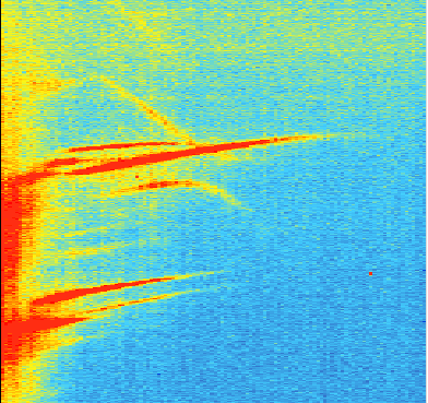
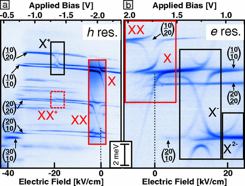
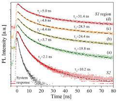
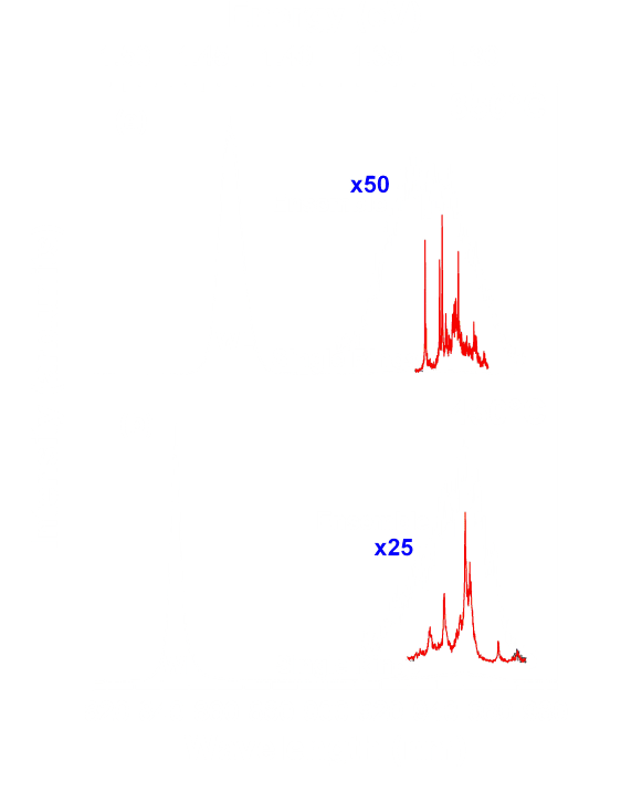
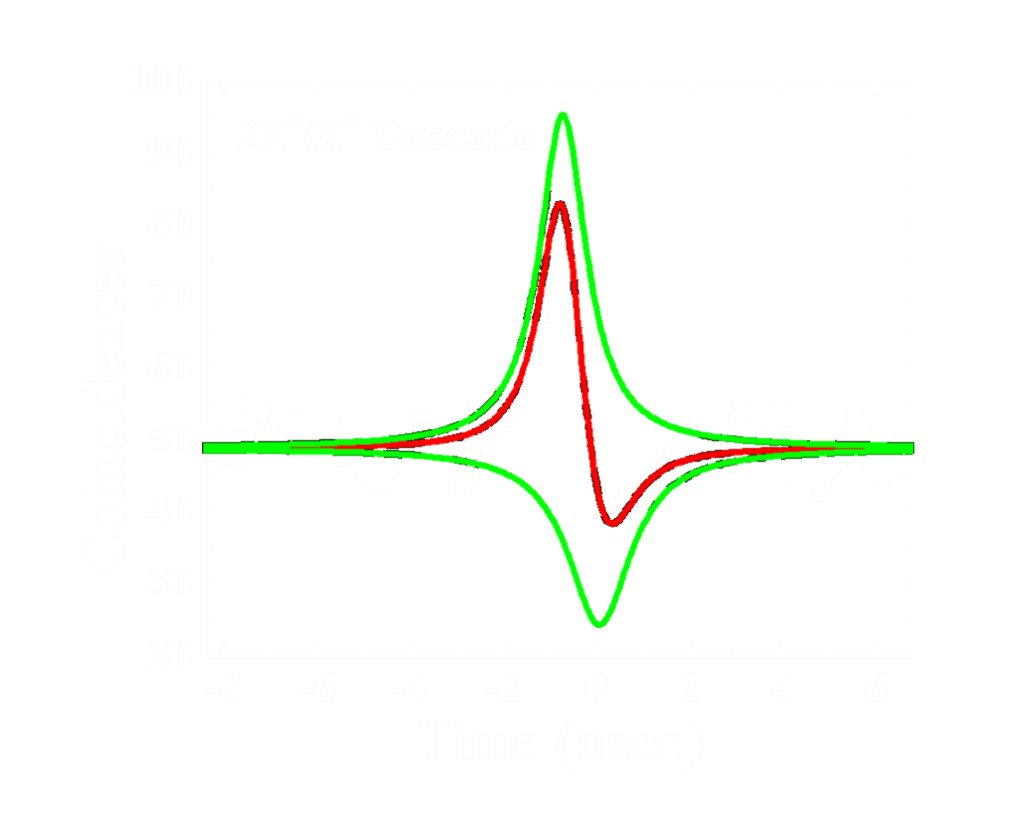
Photon Correlation Measurements

Quantum dots may serve as single photon emitters for quantum information technologies. It has also been demonstrated that entangled photon emission is possible. This goal of this research is to generate entangled photon-photon and photon-particle states through optical excitation in coupled quantum dots. The figure shows photon cross-correlation data where the positively charged biexciton followed by the positive trion (2X+/X+) cascade is observed. The 2X+ emission was used as the stop pulse. (Status: Active)

Mobirise

Quantum-confined Stark effects in coupled InAs/GaAs quantum dots

We have observed a continuous and controllable change in the quantum confined Stark effect (QCSE) of excitons in InAs CQDs. The intradot dipole moment was found to vary from approximately the single dot limit for large barriers through zero and ultimately reverse sign for narrow barriers. The maximum value for the Stark shift was found to be ~7.1 ueV/kV•cm-1. The interdot dipole moment is largely linearly dependent on the barrier thickness but shows measurable effects resulting from the molecular nature of the carriers. The interdot exciton was found to have an extremely large Stark shift of up to ~0.97 meV/kV•cm-1, 100 times larger than that of the intradot exciton.
Appl. Phys. Lett. 102, 213101 (2013)

Mobirise

Tunable exciton relaxation in vertically coupled semiconductor InAs quantum dots

Theoretical investigations on the coupling between acoustic phonons and single particle bonding-antibonding states have suggested that orders of magnitude reduction of acoustic phonon scattering rates can be achieved in CQDs. We observed evidence of such a modulation and found that the measured lifetime of the tunable indirect exciton can be understood as a combination of a changing wavefunction distribution, carrier tunneling, and phonon relaxation. We also found that the exciton lifetime can be increased by nearly an order of magnitude.
Phys. Rev. B 84, 081404(R) (2011)

Mobirise

Oscillatory acoustic phonon relaxation of excitons in quantum dot molecules

For the theoretical model for the tunable exciton relaxation, we assume quantum dots with cylindrical symmetry, for which the confinement potentials have been modeled as narrow quantum wells in the growth and in-plane directions matched to parabolic potentials. We focus on the hole scattering rates by bulk acoustic phonons, as these rates are the leading contribution for the neutral indirect exciton relaxation rate when the electron localizes primarily on one dot. The hole–phonon scattering structure factor for acoustic phonons is found to contain a phase relationship between the phonon wave and the hole wave function, which can be tuned by an external electric field. The phase relationship leads to interference effects and tunable oscillatory relaxation rates of indirect excitons, in agreement with experiments.
J. Opt. Soc. Am. B, 29, A146 (2012)

Mobirise

Electric field control of a quantum dot molecule through optical excitation

Nonresonant optical excitation of a coupled quantum dot system was seen to generate a shift in the electric-field-dependent photoluminescence spectra. By monitoring the interdot recombination associated with an electron and hole in different dots we were able to precisely monitor the internal electric field generated. Power, wavelength, and applied field dependence of the charging was studied. Such an optically generated electric field may provide a means for applying local oscillating voltages, allowing for optical tuning of the device parameters.
Appl. Phys. Lett. 96, 211115 (2010)

Mobirise

Photoluminescence Spectroscopy of the Molecular Biexciton in Vertically Stacked InAs-GaAs Quantum Dot Pairs

We present photoluminescence studies of the molecular neutral biexciton-exciton spectra of individual vertically stacked InAs/GaAs quantum dot pairs. We tune either the hole or the electron levels of the two dots into tunneling resonances. The spectra are described well within a few-level, few-particle molecular model. Their properties can be modified broadly by an electric field and by structural design, which makes them highly attractive for controlling nonlinear optical properties.
Phys. Rev. Lett. 99, 197402 (2007)

Mobirise

Optical Signatures of Coupled Quantum Dots

An asymmetric pair of coupled InAs quantum dots is tuned into resonance by applying an electric field so that a single hole forms a coherent molecular wave function. The optical spectrum shows a rich pattern of level anticrossings and crossings that can be understood as a superposition of charge and spin configurations of the two dots. Coulomb interactions shift the molecular resonance of the optically excited state (charged exciton) with respect to the ground state (single charge), enabling light-induced coupling of the quantum dots. This result demonstrates the possibility of optically coupling quantum dots for application in quantum information processing.
Science 311, 636 (2006)

2D Materials

Since the discovery of graphene, new 2D materials are consistently being reported with exceptional characteristics such as extraordinarily high mobilities, semiconducting and superconducting behavior, ferromagnetism, and excellent thermal properties. Many of these materials exhibit optical control of the spin and valley quantum degrees of freedom which may provide novel material-enabled functions in emerging areas such as spintronics and/or valleytronics, providing possible routes to ‘More-than-Moore’

Below are select projects on 2D Materials.

Mobirise

As-grown two-dimensional MoS2 based photodetectors with naturally formed contacts

Scalable fabrication of two-dimensional materials-based devices with consistent characteristics remains a significant impediment in the field. Here, we report on as-grown monolayer MoS2 metal-semiconductor-metal photodetectors produced using a CVD process which results in self-contacted two-dimensional material-based devices. The photodetectors show high responsivity (∼1 A/W) even at a low drain-source voltage (VDS) of 1.5 V and a maximum responsivity of up to 15 A/W when VDS = 4 V with an applied gate voltage of 8 V. The response time of the devices is found to be on the order of 1 μs, an order of magnitude faster than previous reports. These devices demonstrate the potential of this simple, scalable, and reproducible method for creating as-grown two-dimensional materials-based devices with broad implications for basic research and industrial applications.
Appl. Phys. Lett. 110, 261109 (2017)

Mobirise

Concurrent Growth and Formation of Electrically Contacted Monolayer Transition Metal Dichalcogenides on Bulk Metallic Patterns

A process for the growth of self‐contacting monolayers to bulk metallic contacts is reported. Monolayer films, grown on and around patterns of bulk transition metals using chemical vapor deposition, display strong luminescence, monolayer Raman signatures, and relatively large crystal domains, while the metallic patterns provide as‐grown contacts to the material, offering a path for device fabrication and large‐scale production.
Adv. Mater. Interfaces, 4, 1600599 (2017)

Mobirise

Broadband femtosecond transient absorption spectroscopy for a CVD MoS2 monolayer

Carrier dynamics in monolayer MoS2 have been investigated using broadband femtosecond transient absorption spectroscopy (FTAS). A tunable pump pulse was used while a broadband probe pulse revealed ground and excited state carrier dynamics. Interestingly, for pump wavelengths both resonant and nonresonant with the A and B excitons, we observe a broad ground state bleach around 2.9 eV, with decay components similar to A and B. Associating this bleach with the band nesting region between K and Γ in the band structure indicates significant k-space delocalization and overlap among excitonic wave functions identified as A, B, C, and D. Comparison of time dynamics for all features in resonance and nonresonance excitation is consistent with this finding.
Phys. Rev. B 94, 035445 (2016)

Semiconductor Nanostructures

Many properties of nanostructured semiconducting materials can be designed and controlled to enhance their technological impact. For example, the tunable absorption and emission properties of quantum dots are of great interest for many photonic applications and have already been applied to LED devices, biological markers, and nonlinear optical components. While quantum dots, couple extremely well to light, other nanostructures exhibit remarkable electronic transport properties. Combining characteristics from different nanostructures could enable new technologies.

Below are select projects on various Nanostructures.

Mobirise

Optical Properties of a Quantum Dot-Ring System Grown Using Droplet Epitaxy

Electronic and optical properties of InAs/GaAs nanostructures grown by the droplet epitaxy method are studied. Carrier states were determined by k · p theory including effects of strain and In gradient concentration for a model geometry. Wavefunctions are highly localized in the dots. Coulomb and exchange interactions are studied and we found the system is in the strong confinement regime. Microphotoluminescence spectra and lifetimes were calculated and compared with measurements performed on a set of quantum rings in a single sample. Some features of spectra are in good agreement.
Nanoscale Research Letters 11, 309 (2016)

Mobirise

Improved thermal stability and narrowed line width of photoluminescence from InGaN nanorod by ytterbium doping

Nanorod of in situ Yb‐doped InGaN and undoped InGaN have been grown on (0001) sapphire substrates by plasma assisted molecular beam epitaxy (MBE). Selected regions on Yb‐doped InGaN sample show single dominant near band edge emission (NBE) in green, yellow or orange color due to the variation of In content. Temperature dependent PL peak energy of InGaN nanorod shows the characteristic S ‐shaped behavior indicating the presents of strong exciton localization energy in undoped InGaN nanorod. The exciton localization energy reduced significantly after incorporating Yb into InGaN, giving rise to damping of the S‐shape profile amplitude and narrowing of the PL line width from ∼20 meV to ∼12 meV at 11 K. It is proposed that the improved PL thermal stability and the PL line width in Yb‐doped InGaN nanorod is affected by the Yb gettering effect.
Phys. Status Solidi C 12, 413 (2015)

Mobirise

Optical pumping and negative luminescence polarization in charged GaAs quantum dots

Optical pumping of electron spins and negative photoluminescence polarization are observed when interface quantum dots in a GaAs quantum well are excited nonresonantly by circularly polarized light. Both observations can be explained by the formation of long-lived dark excitons through hole spin relaxation in the GaAs quantum well prior to exciton capture. In this model, optical pumping of resident electron spins is caused by capture of dark excitons and recombination in charged quantum dots. Negative polarization results from accumulation of dark excitons in the quantum well and is enhanced by optical pumping. The dark exciton model describes the experimental results very well, including intensity and bias dependence of the photoluminescence polarization and the Hanle effect.
Phys. Rev. B 79, 035322 (2009)

Mobirise

Super Low Density InGaAs Semiconductor Ring-Shaped Nanostructures

Fabrication of super low density InGaAs semiconductor ring-shaped nanocrystals is demonstrated on a GaAs (100) surface by using molecular beam epitaxy. Specifically, densities down to 2.3 × 10^6 cm^−2 are fabricated with only self-assembled methods based on droplet epitaxy. This is several orders of magnitude lower than conventional growth.
Crystal Growth & Design, 8, 1945 (2008)

Mobirise
Mobirise
Mobirise
Mobirise
Address

Clippinger Labs, Room 251
Ohio University
Athens, OH 45701

Contacts

Email: stinaff@ohio.edu
Phone: 740-597-2567                     
Fax: 740-593-0433

© Copyright 2018 Stinaff Lab - All Rights Reserved